by Sharena Rice, contributing editor
February 2023 issue
Neurotechnology researchers have made significant strides in understanding the workings of the brain, but there is still much to learn and to integrate. As patients and clinicians live in a world with changing needs and moving parts, focusing on only one technique or one type of technology has limits. The usefulness of implants has been limited by their interoperability: a person with an implant may be able to communicate, move, or sense far more easily than they could without the implant. Yet implants may scatter light and therefore not be suitable for use in emerging optogenetics applications, which need light to change neural activity. Implants may create artifacts in MRIs, which could prevent clinicians from being able to detect neural dysfunctions. Further, implants must conduct electricity if they need to stimulate and measure from the implanted tissue. Thus, a key challenge in bioelectronic medicine is the integration of solutions for maximal compatibility.
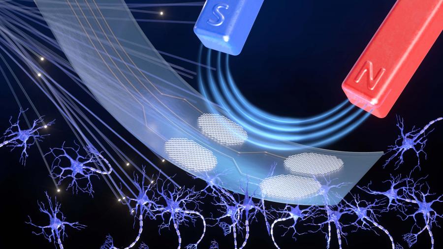
In their paper “Multilayer CVD graphene electrodes using a transfer-free process for the next generation of optically transparent and MRI-compatible neural interfaces,” a team in the Bioelectronics Group at Delft University of Technology described their innovations in building a foundational piece of a multimodal platform. They developed electrodes that are electrically conductive, optically transparent, and MRI-compatible. Graphene, a material that is grown via chemical vapor deposition processes and can be sandwiched between transparent biocompatible polymers, is a suitable candidate for such electrodes. However, the high graphene growth temperature and the presence of polymers have made fabrication difficult, and the manual transfer process of pre-grown graphene sheets has led to reliability issues.
To solve this problem, the team fabricated the chemical vapor deposition-based multilayer graphene electrodes using a wafer-scale transfer-free process, which was specifically designed for use in optically transparent and MRI-compatible neural interfaces. These graphene electrodes exhibited very low impedances, comparable to those of noble metal electrodes of the same size and geometry. The electrodes also exhibited the highest charge storage capacity reported to date among all previously fabricated CVD graphene electrodes.
According to Vasso Giagka, PI of this study, “These electrodes can be mass fabricated and the transfer-free process we introduce here makes the whole process more robust and scale-able. In the future, this process will allow us to introduce further local modifications towards more intelligent implants. The multi-layer nature of our graphene leads to a significant increase in their charge storage capacity compared to their monolayer counterparts, an important property for neurostimulating electrodes.”
The researchers found that their graphene electrodes did not reveal any photo-induced artifact during 10-Hz light pulse illumination. In addition, they demonstrated for the first time that CVD graphene electrodes do not cause image artifacts in a 3 Tesla MRI scanner, so has potential for use in functional neuroimaging to better understand what is happening with the brain both at the area immediately surrounding the implant and in the broader networks of the nervous system. These results demonstrate that multilayer graphene electrodes are excellent candidates for the next generation of neural interfaces and can substitute the standard conventional metal electrodes.
Even beyond their optical properties, the advantages of these graphene electrodes are clear. They enable multimodal neural recording, electrical and optogenetic stimulation, while allowing for optical imaging, as well as artifact-free MRI studies. The low impedance and high charge storage capacity of these electrodes means that they are highly sensitive, allowing for more precise neural recording.
Said Giagka, “Graphene and its derivatives can be modified to fulfill several of these functionalities on a single implant.”
The development of CVD-based multilayer graphene electrodes is useful both as a neuroscience research tool and for the field of bioelectronic medicine. If further developed for wireless powering and further suitability for long-term use, these electrodes may enhance our understanding of the body, enabling new therapies for neurological disorders. The ability to use a single electrode for multiple applications, while maintaining sensitivity and avoiding image artifacts, is not just a step forward with one mode, but a leap forward as a more integrated multimodal solution.
